
From the circuits in everyday gadgets to the sensors that track weather or medical data, the smallest components often have the biggest impact. Microfabrication makes these microscopic marvels possible through techniques that allow engineers to shape materials at an incredibly fine scale. It forms the backbone of many modern technologies, linking science and practicality in every layer. While the process may sound complex, its purpose is simple: to build reliable systems that power today’s connected world.
Understanding the Basics of Microfabrication
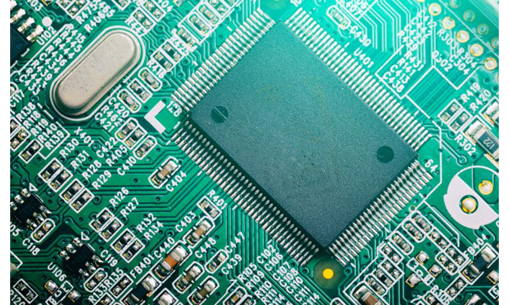
Microfabrication is the process of creating very small structures, usually on the scale of micrometres. It plays a central role in producing components for electronics, sensors, and optical systems. Think of it as the art of building the unseen, where entire circuits or devices are made smaller than the width of a human hair.
The process began with the demand for compact electronics and reliable performance. Over time, it has evolved into a practical toolset used across industries, from medical devices to telecommunications. What makes microfabrication fascinating is how it bridges science and manufacturing, turning complex concepts into tangible, working parts.
How Photolithography Shapes the Process
One of the main techniques behind microfabrication is Photolithography. It uses light to transfer patterns onto a surface coated with a light-sensitive material known as a photoresist. When exposed to ultraviolet light through a patterned mask, the photoresist reacts, allowing precise etching and patterning.
This process may sound like something straight out of a science lab, but it is a daily routine in semiconductor production. Photolithography defines where each transistor or line will appear, ensuring every layer aligns perfectly. It’s like shining a torch through a stencil, but instead of paper, the result becomes the foundation of modern electronics.
Without Photolithography, the chips inside computers, mobile phones, and cameras would not exist in their current form. Its precision allows manufacturers to fit more circuits into smaller areas, improving energy efficiency and performance without exaggerating the feat.
Tools and Materials That Make It Work
Microfabrication relies on cleanroom environments designed to keep contaminants away from sensitive layers. Even a tiny dust particle can compromise a wafer, so the air inside is heavily filtered and tightly controlled. Equipment such as etchers, deposition systems, and microscopes operate with precision to maintain uniform results.
Common materials include silicon, glass, and polymers, chosen for their durability and compatibility with various fabrication processes. Silicon stands out for its reliability and electrical stability, which is why it remains a standard base in electronic manufacturing.
Every step of production, from coating to etching, demands careful supervision. This attention to precision ensures consistent quality, where even the smallest detail can make a big difference.
Why Microfabrication Matters Today
Microfabrication plays a vital role in multiple industries shaping today’s world. In healthcare, it enables lab-on-a-chip devices that can analyse samples with minimal material. In telecommunications, it supports the creation of compact sensors that improve communication speed. Automotive systems also depend on microfabricated parts for safety and performance monitoring.
In the energy sector, micro-scale designs help reduce material use and improve the reliability of electronic systems. This discipline emphasises precision and continuous improvement, with each refinement enhancing how different systems operate together.
The impact of microfabrication extends through nearly every part of modern life. From wearable gadgets to satellites, its quiet influence keeps technology running smoothly and efficiently.
The Role of Photolithography in Future Developments
Photolithography continues to push boundaries as the demand for smaller and faster devices grows. Modern systems use shorter wavelengths of light, allowing even finer patterns. These developments help industries build components with features measured in nanometres.
The method also inspires alternative approaches such as nanoimprint and electron-beam lithography. While each technique differs, the principle remains the same: control light or particles to define structure at an almost invisible scale. The challenge lies in maintaining accuracy while reducing costs and energy use.
Researchers and engineers are also exploring eco-friendly processes, aiming to reduce chemical waste and power consumption. The shift towards sustainability doesn’t mean sacrificing precision; it encourages smarter use of resources. That’s a bright idea in more ways than one.
Everyday Impact of Microfabrication
It’s easy to overlook how much of daily life depends on this technology. Every time someone taps on a smartphone, uses a GPS, or takes a digital photo, there’s a piece of microfabrication at work. Its influence extends to industries people rarely associate with technology, like agriculture, where sensors monitor soil and water quality.
Education and research institutions also benefit, as microfabrication opens new opportunities for students and professionals to create and test prototypes. It’s a quiet revolution built on consistent engineering rather than marketing slogans. The results are visible in the convenience and reliability of the tools people use daily.
A Look Ahead
Microfabrication and Photolithography continue to evolve as the world demands smaller, smarter, and more sustainable technologies. Each advancement brings improved reliability, reduced material use, and new ways to integrate electronics into unexpected areas.
The future may be uncertain, but one thing remains clear: precision manufacturing will always have a place wherever technology meets practicality. Every innovation, no matter how small, starts with a single patterned layer that grows into something bigger. Contact Singapore Epson Industrial to learn more about how advanced manufacturing solutions can support your next project.